The world we live in today is dominated by technology, and at the heart of this technological revolution lies a critical component – Printed Circuit Boards (pcb assembly). These unassuming, yet indispensable boards are the backbone of almost all electronic devices, making PCB fabrication a crucial aspect of modern manufacturing.
The Birth of PCBs: The history of PCBs dates back to the early 20th century, and since then, they have continually evolved. Before PCBs, electronics were interconnected using point-to-point wiring, a time-consuming and error-prone process. The advent of PCBs streamlined this, leading to more efficient and reliable electronic devices.
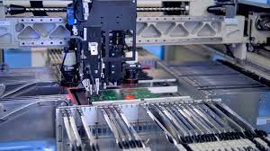
The PCB Fabrication Process: PCB fabrication is a highly intricate process. It begins with the design phase, where engineers create a blueprint of the PCB’s layout, determining the position of components and the routing of electrical connections. This design is then converted into a Gerber file, which serves as a set of instructions for the fabrication process.
Materials and Layering: The next step involves selecting the appropriate materials. PCBs are typically made from various substrates, with fiberglass and epoxy resins being the most common choices. The layers of the board are built up by stacking copper-clad substrates, and the number of layers depends on the complexity of the device. Multi-layer PCBs offer greater flexibility for routing connections.